Package Science Services
IC Packaging Specialists

Call: +1 (800) 218-1573
email: info@pkgscience.com
Package Design
Complete Design Services
PSS can help you select the right package for your IC, SIP or discrete component:
Form Factor
Lead Count
Chip Attachment
Interconnect / Signal and Power Integrity (SI/PI)
Thermal Management
Cost
PSS is familiar with and can design and implement any package type:
Lead-frame including QFN
Laminate: organic multilayer BGA/PGA
Ceramic: multilayer BGA/PGA/LCC
CSP: reroute, UBM, bumping
LCP
SIP: stacked, arrayed, TSV
POP: package stacking
WLP
Flex
Flip chip, wire bond, conductive adhesive
High speed, high power
Design Tools
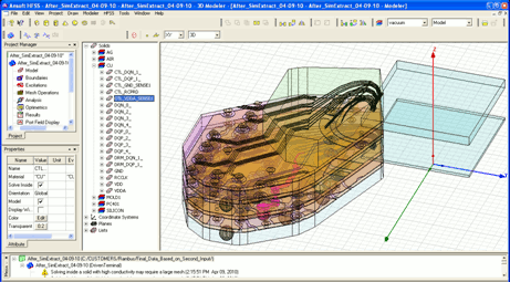
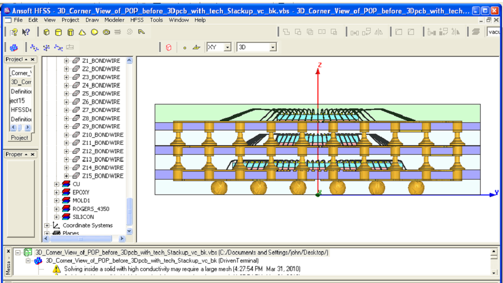
PSS primarily uses CAD Design Software tools to generate manufacturable designs for all package types. Package families from lead frame to high-density BGA's can be designed using CDS Electronic Package Design (EPD). The tool has the ability to generate designs using customer and manufacturing DRC data and maintain netlist integrity across multiple die and packages. Lead frame design is automatic and parametric, allowing fast and accurate design and optimization. Multilayer, stacked and PoP designs use automated, DRC-ruled routines with full manual edit capability. In addition, output utilities allow true 3D entities to be transferred directly into and from CAD/CAM, simulation, analysis and modeling tools. Other tools include Autocad, SolidWorks, Pro-E and PADS PCB. Specific design tools such as Cadence Allegro and Mentor Board Station can be made available upon request.
LED and PV/Solar cell packaging and PCB's are also a specialty of PSS. All LED package types and mounting substrates, PCBs and enclosures are supported by our design team. Domestic and offshore manufacturing is available. Advanced materials and novel design support is available.
Click here for details on IC package design flow.
© 2011 Package Science Services LLC