Package Science Services
IC Packaging Specialists

Void Detection in Underfill
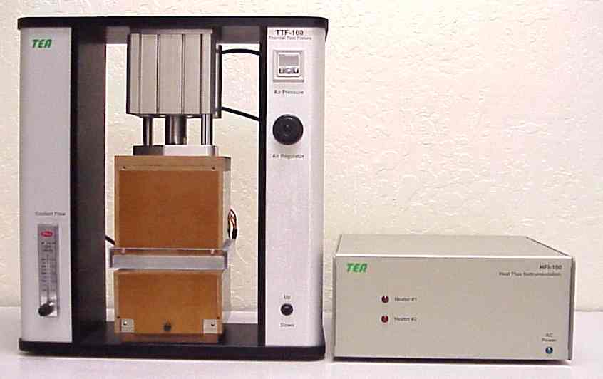
TIM Measurement
Material Temp-Cycle
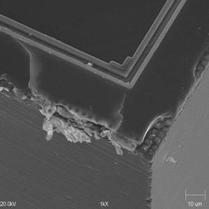
Passivation Damage
Call: +1 (800) 218-1573
email: info@pkgscience.com
Materials, Process, Assembly
Design and Manufacturing
A wide range of materials are used in the manufacture of electronic systems. PSS has helped customers select materials for prototypes, special configurations and products for mass production. A good knowledge of current materials means keeping in touch with major suppliers to match the best material and supply chain to customer specifications. In many cases, the product may be in development or production and a problem with materials may cause defects. Techniques such as acoustic microscopy, x-ray, cross-sections and SEM are used to identify and analyze defects in interface materials, while mechanical modeling and stress analysis are used to evaluate material properties and assembly configurations. Assembly DOE and other methods are used to validate models. Materials are typically selected from commercially available sources to help reduce cost and maintain supply. Our staff keeps abreast of new materials developments throughout the industry via conference attendance and journals. Technical resources include industry and academic contacts working on next-generation materials and processes.
The materials selected must also include consideration for process. Temperature history and process limitations are evaluated for the system from raw materials to final product to support DFM techniques and reduce complexity and cost of the manufacturing proceses.
A few examples of our work:
Flip-chip underfill for low-k
Die attach material and process optimization
Thermal interface material (TIM) analysis and selection
Hi thermal conductivity dielectric analysis
Multi-chip wire bonding
Flip-chip solder and underfill selection
Overmold materials and process for open-cavity encapsulation
Solder process optimization for on-package discrete components
Laser package thermal optimization using new materials
High-temperature device packaging design, material selection
Medical product design and prototype
Package Science has close ties to local assembly houses with expert staff and state-of-the-art facilities This association enables two-way communication with the assembly partners with participation in local technical discussions on existing and emerging technologies as well as access to materials and equipment expertise. US based capacities to thousands per month as well as prototype and sample production runs. Offshore contacts are available for many of the major houses in Asia and Europe to facilitate mass-volume needs.
Materials and Process Areas
Substrate, leadframe, hermetic, organic
Die attach, underfill, overmold
Ceramics, plastics, polymers, metals
Plating, solders, glass and metal sealing
Wire bond, metallization, flip-chip, UBM, pillars
Stacked chip interposers, interlayer materials, TSV
Failure analysis
© 2010 Package Science Services LLC