Package Science Services
IC Packaging Specialists

Call: +1 (800) 218-1573
email: info@pkgscience.com
SERVICES
Package Conceptualization and Selection
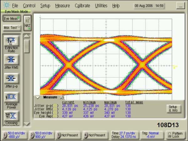
PSS can help you select the right package form factor, lead count, attachment, interconnect type, thermal considerations and cost to fit your product. When designing a device, the package is often disregarded early in the design cycle or is not considered to be a difficult task. But in many cases the package can be the limiting factor in time-to-market, cost and performance if the design is not well thought out and executed. The package form factor, materials and manufacturing methods should be as standard as possible to control costs and available resources in typical cases. For advanced packaging more complex material sets and interconnect schemes may be used to achieve a balance between cost and performance. The technologies used to design and characterize packages is also extendable to PCBs, sockets, connectors, backplane and other electrical structures. Channel modeling and measurements from chip to system including PCIe, DDR/QDR, SATA, SERDES and USB from DC to 50Ghz.
Design
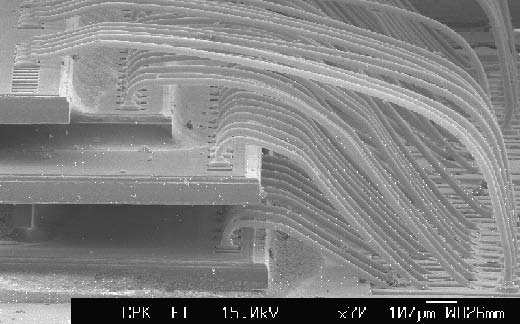
PSS uses sophisticated tools to generate manufacturable designs for all package types including leaded, leadless, array and cavity, flex, SiP, PoP. 3D, and technologies such as through silicon vias (TSV). All package types from lead frame to high-density BGA's can be designed using Cad-Design's Master Foundry Designer Suite. The tool has the ability to generate designs using customer and manufacturing DRC data and maintain netlist integrity across multiple die and packages. Lead frame design is automatic and parametric, allowing fast and accurate design and optimization. Multilayer, stacked and PoP designs use automated, DRC-ruled routines with full manual edit capability. In addition, output utilities allow true 3D entities to be transferred directly into and from CAD/CAM, simulation, analysis and modeling tools. Other tools include Autocad, SolidWorks, Pro-E and PADS PCB. Specific design tools can be made available upon request.
LED and PV/Solar cell packaging and PCB's are also a specialty of PSS. All LED package types and mounting substrates, PCBs and enclosures are supported by our design team. Domestic and offshore manufacturing is available. PSS also has an LED PCB division, LED Package Science.
Modeling, Characterization, Simulation and Analysis
PSS has a wide array of modeling, simulation and measurement tools to predict and verify electrical signal and power integrity, thermal and temperature behavior, and mechanical stress and strain. Measurement capability compliments the modeling and simulation tools. For electrical characterization PSS has capability for time and frequency domain measurements to 50GHz. Full wave and 'quick' 2D and 3D modeling and simulation tools are available as well as power delivery network modeling.
Thermal measurement tools include the capability to measure thermal resistance, material thermal conductivity, contact resistance and accurate multipoint temperature for devices dissipating up to 150W.
Copyright © 2010 Package Science Services LLC
All rights reserved.